# Castellated Breakouts for KiCad
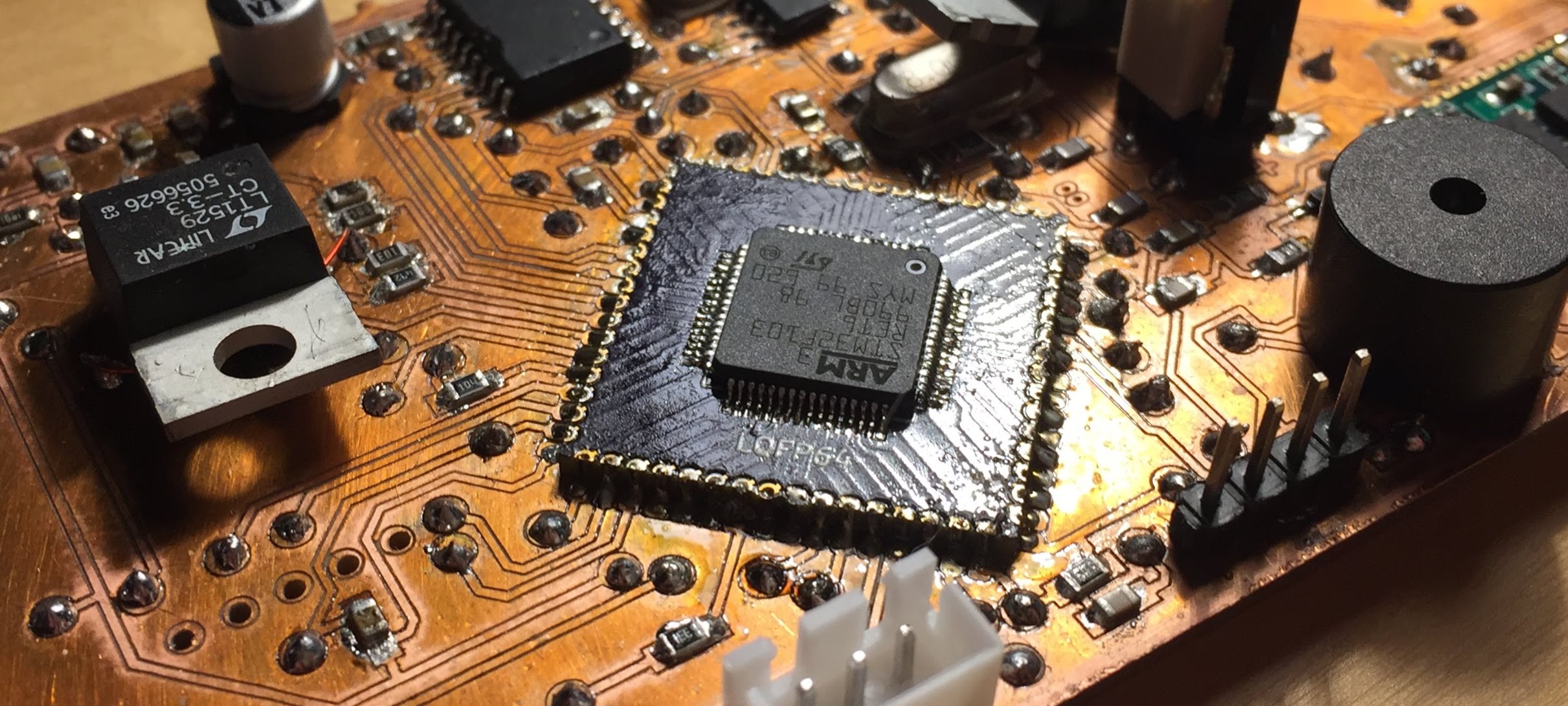
Do you own a milling machine that isn't _quite_ precise enough for that
0.5mm-pitch IC you want to use? Maybe you like to home-etch your PCBs,
but you haven't quite worked out a way of consistently exposing tiny
0.2mm traces? The board designs and footprints in this repository
can help you continue to develop your bespoke hand-crafted electronics
projects at home by letting PCB board houses handle the parts of your
design that are just a little too difficult to be worth fighting with
on your own.
Each board in this repository can be plotted in KiCad and sent off to your
favorite board house (OshPark links are provided below) so you can have
boards for your favorite ICs readily-available for the next time you'd
like to use them in a design.
## Boards
### QFP64 (0.5mm pitch)
 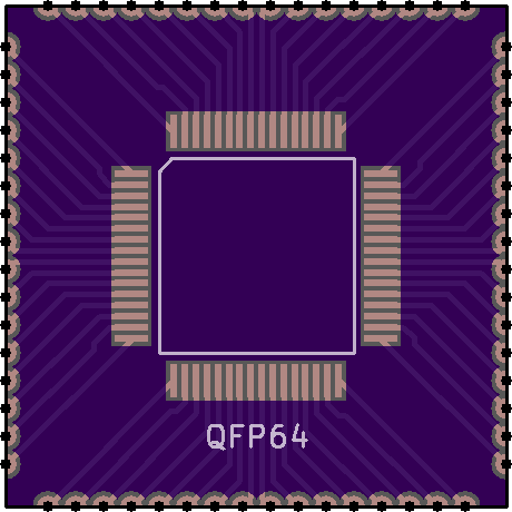
* IC Pin Pitch: 0.5mm
* Compatible packages: QFP64 (BQFP64, CQFP64, LQFP64, TQFP64, etc). No
center pad.
* Castellation Pitch: 1.27mm
* Board Files: [qfp64_0.5mm](qfp64_0.5mm)
### QFP48 (0.5mm pitch)

* IC Pin Pitch: 0.5mm
* Compatible packages: QFP64 (BQFP64, CQFP64, LQFP64, TQFP64, etc). No
center pad.
* Castellation Pitch: 1.27mm
* Board Files: [qfp64_0.5mm](qfp64_0.5mm)
### QFP48 (0.5mm pitch)
 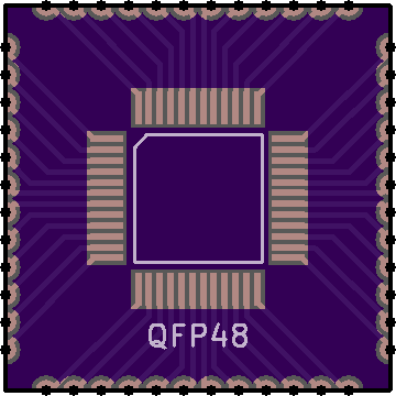
* IC Pin Pitch: 0.5mm
* Compatible packages: QFP48 (BQFP48, CQFP48, LQFP48, TQFP48, etc). No
center pad.
* Castellation Pitch: 1.27mm
* Board Files: [qfp48_0.5mm](qfp48_0.5mm)
### SSOP20 (0.65mm pitch)
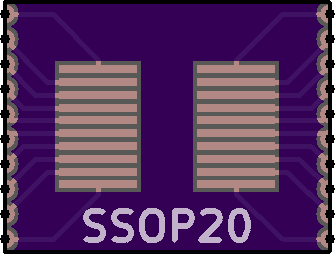
* IC Pin Pitch: 0.65mm
* Compatible packages: SSOP20 (TSSOP20, etc) having a width (including pins)
smaller than 11mm, and having at least 3mm of space available between the
two rows of pins.
* Castellation Pitch: 1.27mm
* Board Files [ssop20_0.65mm](ssop20_0.65mm)
### SSOP8 (0.65mm pitch)
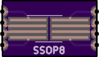
* IC Pin Pitch: 0.65mm
* Compatible packages: SSOP8 (TSSOP8, etc) having a width (including pins)
smaller than 9mm. No center pad.
* Castellation Pitch: 1.27mm
* Board Files: [ssop8_0.65mm](ssop8_0.65mm)
## Plotting
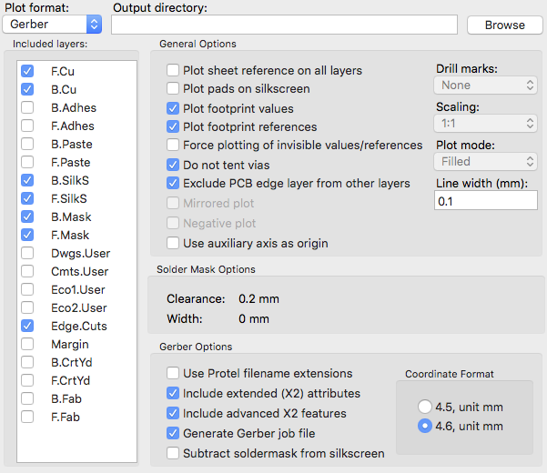
You can plot these on your own in KiCad, just make sure that you do *not*
tent vias. The way castellations are implemented for at least OshPark
involve having vias on the edge of the board, and routing the board
board outline through the center of those vias. If the vias were
tented, you would not be able to easily solder to them!
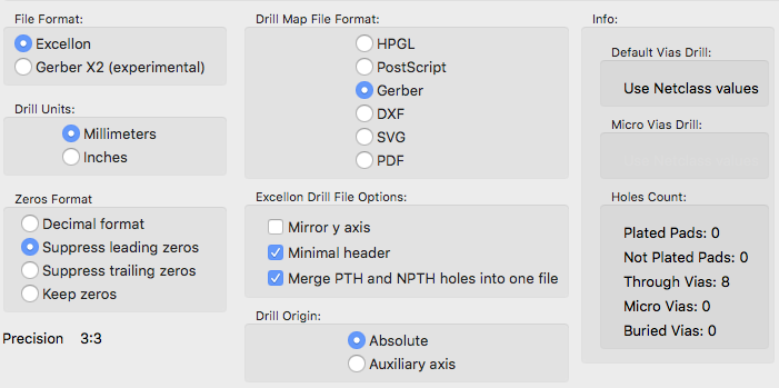
For reference, the settings I've used in generating my plots for OshPark
are below:
### Copper
### Drill
## Contribution Guidelines
This is by no means a prescriptive rule, but if you do find yourself attempting
to contribute a new board or footprint, you may replicate the via spacing
and trace sizes I've used above by configuring your design rules as so:
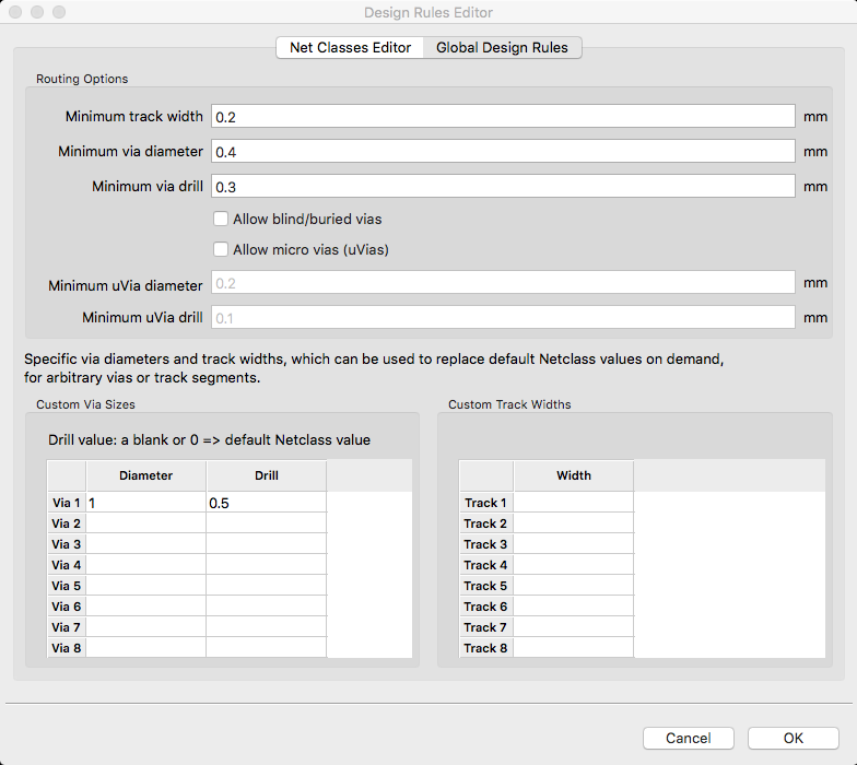
Note that you will want to select the custom via setting (1mm diameter with 0.5mm drill)
when placing the castellation vias.
Matching the patterns used for other footprints is _not_ absolutely necessary,
but if you submit a new breakout board, please try to follow the following
guidelines:
* Place your project in a folder named by the following pattern: `_`,
where `` is the name of the footprint type (`QFN`, `QFP`, `SSOP`) with as general of
a name as possible (that is, exclude prefixes that affect only the height of the package --
suffixes like `T` or `L`, for example), `` is the total count of pins, and ``
is the pin pitch (with units -- millimeters preferred).
* Update the reademe to include a section similar to the sections you see above including:
* A title identifying your new castellated board.
* A bulleted list describing the following details:
* The pin pitch of the footprint.
* A list of common compatible packages including whether the footprint
includes a center pad.
* The pitch of castellations.
* A link to the folder in which you've placed your project's board files.
* (Optional) A link to an OshPark project for that footprint.
* (Optional) An image, preferably from the OshPark preview, of the front
copper layer of the breakout board. Note that you need not host the
image -- as part of merging your PR, the image will be moved to this
project's folder in S3.
## Disclaimer
I am a hobbyist -- not an expert! If you see a problem in the design of
any linked boards or have suggestions that might make this project more
useful, I'd love to hear them!

* IC Pin Pitch: 0.5mm
* Compatible packages: QFP48 (BQFP48, CQFP48, LQFP48, TQFP48, etc). No
center pad.
* Castellation Pitch: 1.27mm
* Board Files: [qfp48_0.5mm](qfp48_0.5mm)
### SSOP20 (0.65mm pitch)

* IC Pin Pitch: 0.65mm
* Compatible packages: SSOP20 (TSSOP20, etc) having a width (including pins)
smaller than 11mm, and having at least 3mm of space available between the
two rows of pins.
* Castellation Pitch: 1.27mm
* Board Files [ssop20_0.65mm](ssop20_0.65mm)
### SSOP8 (0.65mm pitch)

* IC Pin Pitch: 0.65mm
* Compatible packages: SSOP8 (TSSOP8, etc) having a width (including pins)
smaller than 9mm. No center pad.
* Castellation Pitch: 1.27mm
* Board Files: [ssop8_0.65mm](ssop8_0.65mm)
## Plotting
You can plot these on your own in KiCad, just make sure that you do *not*
tent vias. The way castellations are implemented for at least OshPark
involve having vias on the edge of the board, and routing the board
board outline through the center of those vias. If the vias were
tented, you would not be able to easily solder to them!
For reference, the settings I've used in generating my plots for OshPark
are below:
### Copper

### Drill

## Contribution Guidelines
This is by no means a prescriptive rule, but if you do find yourself attempting
to contribute a new board or footprint, you may replicate the via spacing
and trace sizes I've used above by configuring your design rules as so:

Note that you will want to select the custom via setting (1mm diameter with 0.5mm drill)
when placing the castellation vias.
Matching the patterns used for other footprints is _not_ absolutely necessary,
but if you submit a new breakout board, please try to follow the following
guidelines:
* Place your project in a folder named by the following pattern: `_`,
where `` is the name of the footprint type (`QFN`, `QFP`, `SSOP`) with as general of
a name as possible (that is, exclude prefixes that affect only the height of the package --
suffixes like `T` or `L`, for example), `` is the total count of pins, and ``
is the pin pitch (with units -- millimeters preferred).
* Update the reademe to include a section similar to the sections you see above including:
* A title identifying your new castellated board.
* A bulleted list describing the following details:
* The pin pitch of the footprint.
* A list of common compatible packages including whether the footprint
includes a center pad.
* The pitch of castellations.
* A link to the folder in which you've placed your project's board files.
* (Optional) A link to an OshPark project for that footprint.
* (Optional) An image, preferably from the OshPark preview, of the front
copper layer of the breakout board. Note that you need not host the
image -- as part of merging your PR, the image will be moved to this
project's folder in S3.
## Disclaimer
I am a hobbyist -- not an expert! If you see a problem in the design of
any linked boards or have suggestions that might make this project more
useful, I'd love to hear them!